Latest News

NANOSENSORS Meet NANOSENSORS at booth 218 at ChinaNano 2019 Beijing August 17... - news

Meet NANOSENSORS at booth 218 at ChinaNano 2019 Beijing August 17...Sat Aug 17 2019

We are at booth 218 at the ChinaNano 2019, the 8th International Conference on Nanoscience and Technology at the Beijing International Convention Center (BICC). We are looking forward to seeing you there! Learn all about NANOSENSORS AFM probes at the... #AFMcantilever
#AFMProbes #AFMprobes

NANOSENSORS NANOSENSORS proudly sponsors Asia-Pacific PFM 2019 workshop - news

NANOSENSORS proudly sponsors Asia-Pacific PFM 2019 workshopMon Aug 12 2019

Published new post (NANOSENSORS proudly sponsors Asia-Pacific PFM 2019 workshop) on NANOSENSORS Blog NANOSENSORS™ is a proud sponsor of the 2019 Asia-Pacific Workshop on Piezoresponse Force Microscopy ( PFM) and Nanoscale Electromechanics of Functional Materials and Electrochemical Systems (Asia-Pacific PFM 2019), which will be held in Seoul, Republic of Korea, from August 11 to 14, 2019. We wish all those members of the #AFMcommunity who are participating this week a successful workshop. In the NANOSENSORS blog you will regularly find references to articles mentioning the use of our AFM probes for Piezoresponse Force Microscopy. You’re welcome to have a look at: https://www.nanosensors.com/blog/tag/pfm/ #PiezoresponseForceMicroscopy #nanoscale #materials

NanoWorld Effect of Staple Age on DNA Origami Nanostructure Assembly and Stability - news

Effect of Staple Age on DNA Origami Nanostructure Assembly and StabilityMon Aug 12 2019

Effect of Staple Age on DNA Origami Nanostructure Assembly and Stability (https://www.nanoworld.com/blog/effect-of-staple-age-on-dna-origami-nanostructure-assembly-and-stability/?utm_source=Facebook&utm_medium=Blog&utm_content=Effect+of+Staple+Age+on+DNA+Origami+Nanostructure+Assembly+and+Stability&utm_campaign=NanoWorld+Blog) has been published on NanoWorld Blog. DNA origami nanostructures are widely employed in various areas of fundamental and applied research. Due to the tremendous success of the DNA origami technique in the academic field, considerable efforts currently aim at the translation of this technology from a laboratory setting to real-world applications, such as nanoelectronics, drug delivery, and biosensing. While many of these real-world applications rely on an intact DNA origami shape, they often also subject the DNA origami nanostructures to rather harsh and potentially damaging environmental and processing conditions.* In their article “Effect of Staple Age on DNA Origami Nanostructure Assembly and Stability” Charlotte Kielar, Yang Xin, Xiaodan Xu, Siqi Zhu, Nelli Gorin , Guido Grundmeier, Christin Möser, David M. Smith and Adrian Keller investigate the effect of long-term storage of the employed staple strands on DNA origami assembly and stability.* Atomic force microscopy (AFM) under liquid and dry conditions was employed to characterize the structural integrity of Rothemund triangles assembled from different staple sets that have been stored at −20 °C for up to 43 months.* NanoWorld Ultra-Short Cantilevers USC-F0.3-k0.3 were the AFM probes that were used for the AFM measurements under liquid conditions.* https://www.nanoworld.com/Ultra-Short-Cantilevers-USC-F0.3-k0.3.html Please have a look at the NanoWorld blog for the full citation and a direct link to the full article. #DNA #nanotechnology #AtomicForceMicroscopy

NANOSENSORS Nucleation in confinement generates long-range repulsion between rough calcite surfaces - news

Nucleation in confinement generates long-range repulsion between rough calcite surfacesMon Aug 05 2019

Nucleation in confinement generates long-range repulsion between rough calcite surfaces on NANOSENSORS™ Blog Fluid-induced alteration of rocks and mineral-based materials often starts at confined mineral interfaces where nm-thick water films can persist even at high overburden pressures and at low vapor pressures. These films enable transport of reactants and affect forces acting between mineral surfaces. However, the feedback between the surface forces and reactivity of confined solids is not fully understood.* In “Nucleation in confinement generates long-range repulsion between rough calcite surfaces» Joanna Dziadkowiec, Bahareh Zareeipolgardani, Dag Kristian Dysthe and Anja Røyne describe how they used the surface forces apparatus (SFA) to follow surface reactivity in confinement and measure nm-range forces between two rough calcite surfaces in NaCl, CaCl2, or MgCl2 solutions with ionic strength of 0.01, 0.1 or 1 M.* Roughness evolution with time of single, unconfined calcite films in salt solutions was analyzed by Atomic Force Microscopy using NANOSENSORS™ uniqprobe qp-SCONT AFM probes to image the surfaces in contact mode.* https://www.nanosensors.com/uniqprobe-uniform-quality-spm-probe-soft-contact-mode-qp-scont Please have a look at the NANOSENSORS™ blog for the full citation and a direct link to the full article. #AtomicForceMicroscopy #ChemicalPhysics #RoughnessCharacterization

NanoAndMore The Skeptics' Guide to the Universe - news

The Skeptics' Guide to the UniverseFri Aug 02 2019

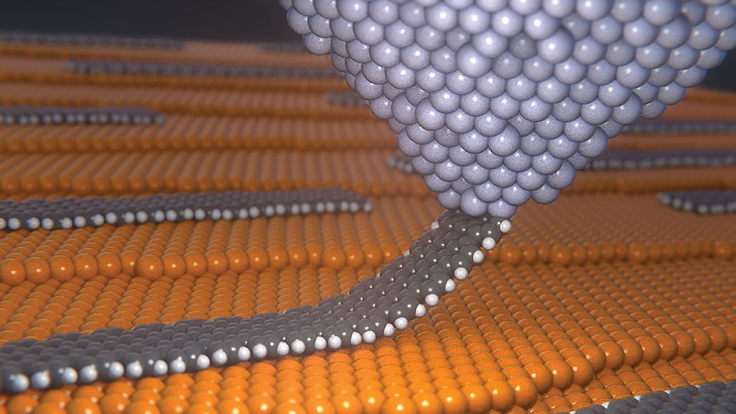
Friction is everywhere — from a violinist bowing a string to children skidding down a slide. In the right situation, the ubiquitous force can have big effects: Interleave the pages of two phone books, and the friction between the pages will hold the books together so tightly that they become strong enough to suspend a car above the ground.

NanoWorld Happy Birthday Switzerland - news

Happy Birthday SwitzerlandThu Aug 01 2019

Happy Birthday Switzerland (https://www.nanoworld.com/blog/happy-birthday-switzerland/?utm_source=Facebook&utm_medium=Blog&utm_content=Happy+Birthday+Switzerland&utm_campaign=NanoWorld+Blog) has been published on NanoWorld Blog. It's the Swiss National Holiday today. Have fun everyone!

NANOSENSORS Happy Swiss National Holiday with Smallest Swiss Cross - news

Happy Swiss National Holiday with Smallest Swiss CrossWed Jul 31 2019

Happy Swiss National Holiday with Smallest Swiss Cross on NANOSENSORS™ Blog Basel University: Smallest Swiss Cross - Made of 20 Single Atoms ( a NANOSENSORS™ PPP-NCL was used for this image) 20 bromine atoms positioned on a sodium chloride surface using the tip of an atomic force microscope at room temperature, creating a Swiss cross with the size of 5.6nm. The structure is stable at room temperature and was achieved by exchanging chlorine with bromine atoms. (Fig: University of Basel, Department of Physics)

NanoWorld Ultra-high resolution imaging of thin films and single strands of polythiophene using atomic force microscopy - news

Ultra-high resolution imaging of thin films and single strands of polythiophene using atomic force microscopyMon Jul 29 2019

Ultra-high resolution imaging of thin films and single strands of polythiophene using atomic force microscopy (https://www.nanoworld.com/blog/ultra-high-resolution-imaging-of-thin-films-and-single-strands-of-polythiophene-using-atomic-force-microscopy/?utm_source=Facebook&utm_medium=Blog&utm_content=Ultra-high+resolution+imaging+of+thin+films+and+single+strands+of+polythiophene+using+atomic+force+microscopy&utm_campaign=NanoWorld+Blog) has been published on NanoWorld Blog. Real-space images of polymers with sub-molecular resolution could provide valuable insights into the relationship between morphology and functionality of polymer optoelectronic devices, but their acquisition is problematic due to perceived limitations in atomic force microscopy (AFM).* In the article “Ultra-high resolution imaging of thin films and single strands of polythiophene using atomic force microscopy” Vladimir V. Korolkov, Alex Summerfield, Alanna Murphy, David B. Amabilino, Kenji Watanabe, Takashi Taniguchi and Peter H. Beton show that individual thiophene units and the lattice of semicrystalline spin-coated films of polythiophenes (PTs) may be resolved using AFM under ambient conditions through the low-amplitude (≤ 1 nm) excitation of higher eigenmodes of a cantilever.* They authors demonstrate that the use of higher eigenmodes in tapping-mode ambient AFM can be successfully employed to characterize both individual polymer strands down to a single-atom level and also the ordering of a semi-crystalline polymer with technological relevance. The combination of AFM and solution deposition provides a simple and high-resolution approach to characterizing the structure of polymers.* The use of NanoWorld Arrow-UHF high frequency AFM probes at their first eigenmode of ~1.4 MHz is mentioned.* https://www.nanoworld.com/ultra-high-frequency-tapping-mode-afm-tip-arrow-uhf Please have a look at the NanoWorld blogpost for the full citation and a direct link to the full article. #AtomicForceMicroscopy #ImagingTechniques #MolecularSelfAssembly

BudgetSensors SEM image of CS-20NG AFN calibration nanogrid standard

BudgetSensors® HS or CS calibration grating!Mon Jul 22 2019

Get the most out of your BudgetSensors® HS or CS calibration grating! No surface is ideally smooth at the nanoscale, but that does not mean you cannot achieve highly accurate and precise calibration. Averaging the scan profile over several micrometers significantly improves your system's calibration. Check out our calibration gratings here: https://www.budgetsensors.com/calibration-standards 

NANOSENSORS Ferroelectricity-free lead halide perovskites – NANOSENSORS™ - news

Ferroelectricity-free lead halide perovskites – NANOSENSORS™Sun Jul 21 2019

Ferroelectricity-free lead halide perovskites on NANOSENSORS Blog. In the recent publication “Ferroelectricity-free lead halide perovskites” Andrés Gómez, Qiong Wang, Alejandro R. Goñi, Mariano Campoy-Quilesa and Antonio Abate describe how they employed direct piezoelectric force microscopy ( DPFM ) to examine whether or not lead halide perovskites exhibit ferroelectricity.* Their article aims to provide a deeper understanding of the fundamental physical properties of the organic–inorganic lead halide perovskites and solves a longstanding dispute about their non-ferroelectric character: an issue of high relevance for optoelectronic and photovoltaic applications.* In the course of their research in which besides using DPFM, they also employed piezoelectric force microscopy ( PFM ) and electrostatic force microscopy ( EFM ), they could demonstrate the non-ferroelectricity of lead halide perovskites. * The PFM images were acquired using a PtIr coated NANOSENSORS PPP-EFM AFM probe. https://www.nanosensors.com/PointProbe-Plus-Electrostatic-Force-Microscopy-PtIr5-Coating-afm-tip-PPP-EFM Please have a look at the NANOSENORS blog for the full citation and a direct link to the full article. #perovskite #photovoltaics #ElectrostaticForceMicroscopy #AFMprobes


Loading
nanosensors-logo
nanoworld-logo
budgetsensors-logo
mikromasch-logo
opus-logo
nanotools-logo